
A new photonic, functional memory based on tin oxide slanted nanorod arrays in which both the optical and electrical stimuli can be used to modulate switching characteristics shows potential for developing high-density and high-efficiency computing systems.
Currently, various research groups worldwide are designing and realizing non-volatile, ultrafast, reliable, functional memory systems that outperform traditional silicon-based flash memories. In this big data era, a new class of data storage devices that can overcome the physical limitations of the existing memory technologies is being pursued vigorously. One such class of memories is commonly known as memristor (an acronym for memory resistor), which can store and process data through electrical signals.
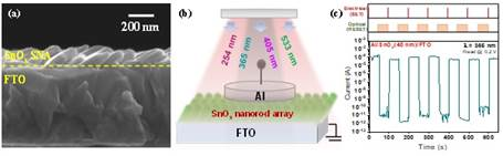
Recently, researchers from the Centre for Nano and Soft Matter Sciences (CeNS), Bangalore, an autonomous institution of the Department of Science and Technology (DST), Govt. of India, have designed such a functional memory based on tin oxide slanted nanorod arrays that shows great potential for the development of high-density and high-efficient computing systems. In this restive memory (non-linear passive two-terminal electrical component which changes its internal resistance between high and low resistance states), both the optical and electrical stimuli can be used to modulate the switching characteristics, including multilevel cell operation.
The CeNS team consisting of Swathi S. P., Athira M., and S. Angappane developed the photonic memory in which the tin oxide slanted nanorod arrays are used as an active layer. The tin oxide nanostructures are prepared by electron-beam evaporation through a technique called the glancing angle deposition (GLAD) technique.
The electron-beam evaporation is a physical vapor deposition method wherein a focussed electron beam is made to bombard the desired target material, which results in its vaporization, and, eventually, deposition of the target material onto the substrate. GLAD facilitates the preparation of complex nanostructures by manipulating the coordinates (tilt and rotation) of the substrate.
The researchers observed good switching characteristics of the memory devices, including low operating voltages, moderate ON/OFF ratio (refers to the ratio of current in the ON state (low resistance state–LRS) to the OFF state (high resistance state- HRS) of the memory device), longer endurance, and better retention with a self-compliance effect in the dark. Interestingly, an unusual negative photo response with an enlarged ON/OFF ratio of greater than 107 and a faster response time is observed under illumination ranging from ultraviolet (254 and 365 nm) to visible light (405 and 533 nm).


